Compound semiconductor photovoltaics
Cu(In1–x,Gax)Se2 (CIGS) is an excellent material for the application to thin-film solar cells. Laboratory-scale cells based on CIGS with efficiencies exceeding 20% have been devised. To enhance the performance of CIGS solar cells and match its device parameters to those of single-crystalline cells (e.g., Si, GaAs), it is necessary to understand the carrier recombination mechanism. The next generation of high-performance solar cells will require high-quality CIGS films with even higher Ga concentrations since the ideal bandgap energy for a single junction solar cell is predicted to be 1.4–1.5 eV, which corresponds to x = ~0.7. Eliminating defects in CIGS is necessary to improve the film quality and reduce carrier recombination in solar cells. A great deal of study on defect properties in CIGS, such as density of states and influence on device performances, has been carried out in this decade. Nevertheless, defect features in CIGS films, especially at high Ga concentrations, are not yet clearly understood due to the fluctuation in its optoelectronic properties, complex device structures, and multinary composition. Thus, a systematic study of defects in CIGS is necessary for the efficient production of the high-quality thin-films. So, we are investigating the defects in CIGS using various structural (X-ray diffraction, raman scattering, and positron annihilation), electrical (current-voltage, admittance, and photocapacitance), and optical (photo-luminescence, TW-PL, etc.) characterization techniques.
Photocatalysts
Solar water splitting using semiconductor based photocatalyst is a effective route for the production of H2, which can be used as a clean fuel, a sustainable and environmentally energy source. Semiconductors are particularly useful as photocatalysts because of a favorable electronic structure, light absorption properties, and charge transport properties etc. In our laboratory, we focus on Bismuth vanadate (BiVO4), an n-type metal oxide semiconductor, which become a potential photoanode for O2 production through water-splitting, and also for H2 production making Z-scheme structure in conjucntion with other p-type semiconductor. We focus research on the deposition of doped BiVO4 thin film or the enhancement of photoactivities with improved carrier transport properties. We investigate optical and electrical properties using Raman spectroscopy, time-resolved photoluminescence, impedance spectroscopy etc. Crystal structures are studied suing XRD and X-ray Rietveld refinement method.
Widegap Semiconductors
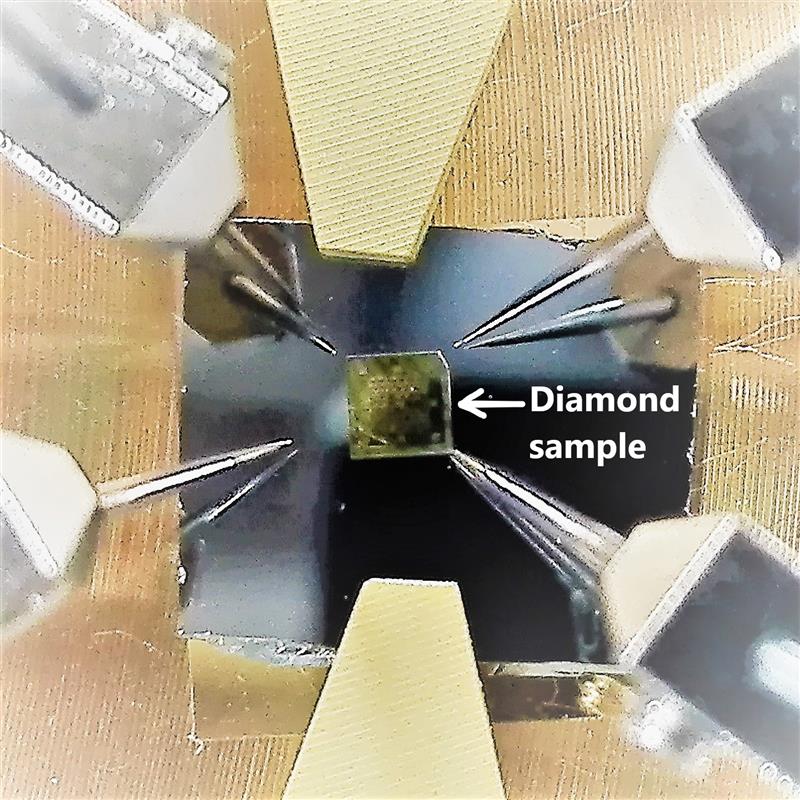
Semiconducting diamond is intensively investigated worldwide for wide range of applications, including quantum devices, magnetics field sensing, and power-electronics. Diamond is composed of carbon and can be synthetized by using a gas mixture of methane and hydrogen (Chemical Vapor Deposition “CVD” process). Nowadays, most of basic solid-state electronic devices such as Schottky diode, p-i-n diode, MOSFET, MOSFET, and JFET can be fabricated by using diamond material. Given its outstanding electrical and thermal properties such as a breakdown electrical strength of 10 MV/cm (30 times that of Silicon) and an unsurpassed thermal conductivity (22 W/mK), diamond devices are expected to outperform the silicon technologies, and offer great performance advantages in high power applications. On the other hand, the unique characteristics of single defects of diamond such as nitrogen-vacancy complexes (NV centers) offer immense potential for magnetics field sensing and quantum computers applications. Negatively charged NV centers exhibits red fluorescence (causes by a green laser irradiation) and electron spin that are mainly exploited in these applications.
In our laboratory, we focus on the study of diamond solid-state physics and properties of single defects in diamond. Optical and electrical properties of diamond unipolar devices (Schottky diode, MOSFET), diamond bipolar devices (pin diodes), and single defects in diamond are investigated using various experiments: impedance spectroscopy, photo-capacitance, photoluminescence, optically detected magnetic resonance ODMR, etc.
Organic Semiconductors
The development of organic electronics progressed rapidly in this decade and organic solar cells (OSCs) are regarded as one of the future high potential molecular electronic applications with the advantage of low cost production of printable and flexible devices. One of the approaches for achieving high-performance OSCs is controlling the structural properties of organic semiconductor films, such as grain size and molecular orientation, as these properties directly affect their optical and electrical properties. It is well known that the structural properties of organic semiconductor films are dominated by a delicate balance of molecule-molecule and molecule-substrate interactions. Further, the surface modification technique is useful for controlling the organic film growth processes. In our lab., structural control of OSCs using surface modification techniques has been investigated. Another approach is modification of electric properties at interfaces (organic/organic, organic/inorganic). In organic solar cells (OSCs), an interface exists between the organic molecules and the electrode made of an inorganic material; the electrical properties of this interface affect the performance of the cells. One of the methods used to improve the electrical properties of an interface is to introduce a buffer layer between the organic molecules and the electrode. In heterojunction OSCs composed of phthalocyanine and C60, bathocuproine (BCP) is used as a buffer layer between C60 and metal cathode to improve the cell efficiency. The role of the BCP buffer layer, however, has not been clearly understood yet. In our lab., the influence of the electronic structure of the C60/BCP/metal hetero-interface on the performance of OSCs has been investigated using photoemission spectroscopy techniques (UPS, XPS, etc.).