|
Fujita-Ito Lab. GraduateSchool of Pure and Applied science Institute of Applied Physics, University of Tsukuba |
>>>Japanese |
 Research activity Research activityIntroduction 1. Graphene synthesis 1.1.Graphene FET 1.2.Graphene nano-ribbon 1.3.Three-dimensional nanoporous graphene 1.4.Three-dimensional nanoporous graphene for hydrogen evolution 2.CNT super-capacitor 3.Construction in TEM 3.1.modifing carbon structure 3.2.Pulse induced Fullerene 3.3.Observation of Ga reaction 4.Ultra-sharp probe 5.Visualization of local E-field 6.EB/FIB-CVD technique 7.Carbon nanotube Projects and Funds |
Introduction Graphene is one-atom-thick planar sheets of carbon atoms where the sp2 covalent bond of carbon constructed a hexagonal (honeycomb) crystal lattice. This hexagonal lattice produced superior mechanical and electrical characteristics; the Young's modulus of graphene exceeds 1TPa, and the theoretical electron mobility of 200000 cm2/Vs is about 100 times faster than that of Si. Graphene is a semi-metal material, but one will be able to control the band gap of graphene nanoribbon (GNR) if the width of the GNR would be reduced truly in nanometer sized with the fluctuation of single atomic lattice, on the analogy of the thickness dependency of the band gap in carbon nanotube (CNT). In addition the ideal zigzag edge of GNR should induce so called edge state and a localized spin. The spin orbital interaction on a graphene is expected to be remarkably weak even at a room temperature, thus the long spin-coherent length of graphene will give us a large benefit for the application of spintronics. On the other hand, highly transparent and well conducting thin film is strongly demanded for the surface electrode of solar cells and touch panels. The thin films made from graphene exactly satisfy such requirements and gives wide freedom in the device designing. In addition, the production cost of the graphene film will be much acceptable than that for conventionally utilized transparent film of Indium-Titanium-Oxide (ITO). Our Fujita Lab. has been working on carbon based materials widely from the basis of the mater physics to the device application, through the structural analysis with SEM and HR-TEM observation combined with our home made atom manipulation system. Now our research activity will be categorized into following three themes; 
 1. Graphene synthesis and device application We found that gallium has a unique graphitizing ability to produce a graphene at a very narrow interface between liquid gallium and solid amorphous carbon. It is well known that metal catalyst such as Fe and Ni is commonly utilized to synthesize carbon nanotube (CNT) and/or graphene. The source material of carbon once dissolved into the metal, but an over saturated carbon recrystallized and grew as carbon nanotubes. This precipitation of the excessed carbon sometimes resulted in a nasty problem of multi-layered graphene fragments. Therefore, people frequently used copper as the catalyst for graphene in the recent trend of chemical vapor deposition (CVD) growth technique. The solubility of carbon into copper is quite low, which is about 0.01w%. But, this extremely small solubility strongly limited the reaction area, where the source carbon was soon transformed into a graphene at the surface, and thus the recrystallization was diminished during cooling down process. On the other hand, we uniquely found that liquid gallium also has a nice catalytic ability at the interface with amorphous carbon under vacuum annealing at 1000 oC. Gallium is also well-known as carbon insoluble material, thus the phase diagram of Ga-C system is not available. But, the graphitization of gallium exactly occurred at the interface and graphene was produced. In addition, the liquid nature of gallium shows nice coverage of the surface even if it has certain amount of surface steps and roughness. By using gallium catalyst, we demonstrated FET device operation, where an utra-thin resist channel pattern was transformed into a graphene channel with the gallium. 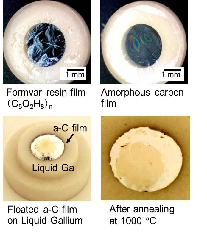
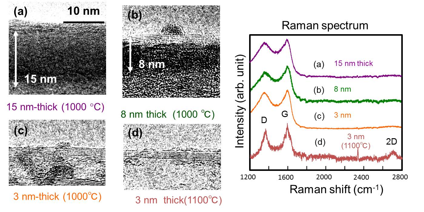
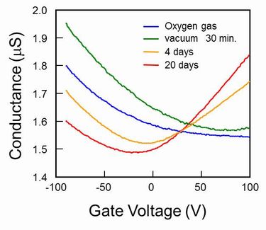
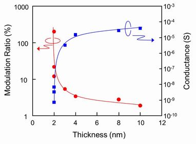
1.1 Graphene FET So called Scotch-Tape method is easy way to prepare a graphene, however, people needed to measure the precise position of the graphene fragment and to pattern source and drain electrode in order to fabricate a back-gate type graphene FET.However, the peering off process of graphene strongly depends on the human handling, thus the poor probability of the device production yield is never applicable for an integrated device circuit. In contrary, our direct transformation of pre-patterned resists film into graphene using the interfacial reaction with gallium can easily be applied to the large scale integration. We prepared an ultra-thin (about 2nm) resist channel pattern on a SiO2 insulated substrate by using electron beam lithography, and graphitized the resist pattern using the gallium. The channel was constructed by a few layers of graphene but the FET showed about 100 % of the maximum conductance modulation was observed at 100 V of the gate biasing voltage. This measurement was done in room atmosphere, thus the adsorbed oxygen on the channel shifted the conductance minima toward the positive biasing region, showing an N type FET characteristic. This size of the graphene channel still be in metallic state, thus the gate biasing could not block the channel conductance. However, we hope that the energy gap that would be opened up by reducing the channel width completely improve the device characteristics for variety of future application. Of course, improvement of the graphene channel quality; how to align the domain direction, and how to reduce the synthesis temperature would be our next urgent issue to be solved. 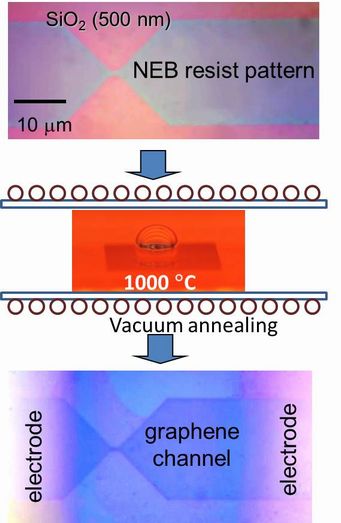
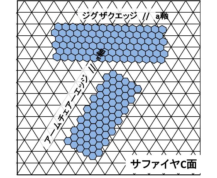
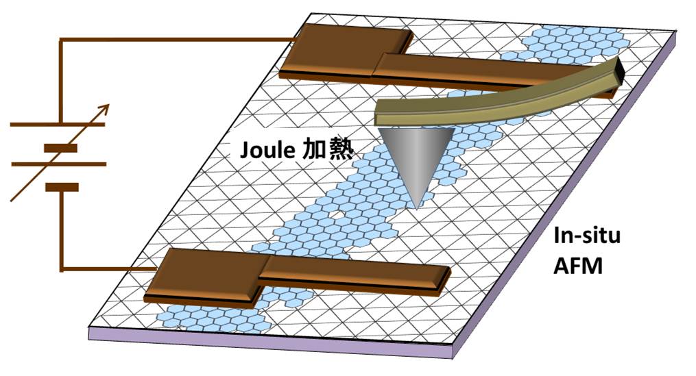
1.2 graphene nanoribbon In order to open up the energy gap on graphene nanoribbon (GNR), we need ultimate reduction of the width of the GNR with a confined edge structure; likewise the electric state of CNT strongly depended both on the width and chirality. Well known technique will be classified into following three ways; However, the resolution limit of an e-beam resist is about 10 nm, containing certain amount of edge roughness due to the polymerization probability, thus the control of the GNR width could not consist with the edge structure control. Zipping of the CNT seems to increase the difficulty when one tries to process a thinner CNT.Cross-linking of polymer, such as coronene and phenylene, seems to have a big advantage to control the edge structure, but the realization of perfect GNR properties has not been reported yet. In this research project, we proposed to use an amyloid protein for the template of the solid state graphitization with gallium. The straight chain polymer of amyloid has about 10 micrometer long and 2 nm to 10nm in diameter, in addition, the shape of the polymer is quite stable in air ambient. Our research undergoes to realize the semiconducting GNR using solid phase graphitization, controlling the GNR's crystal direction as well as the edge structure in relation with the crystallographic direction of the substrate. 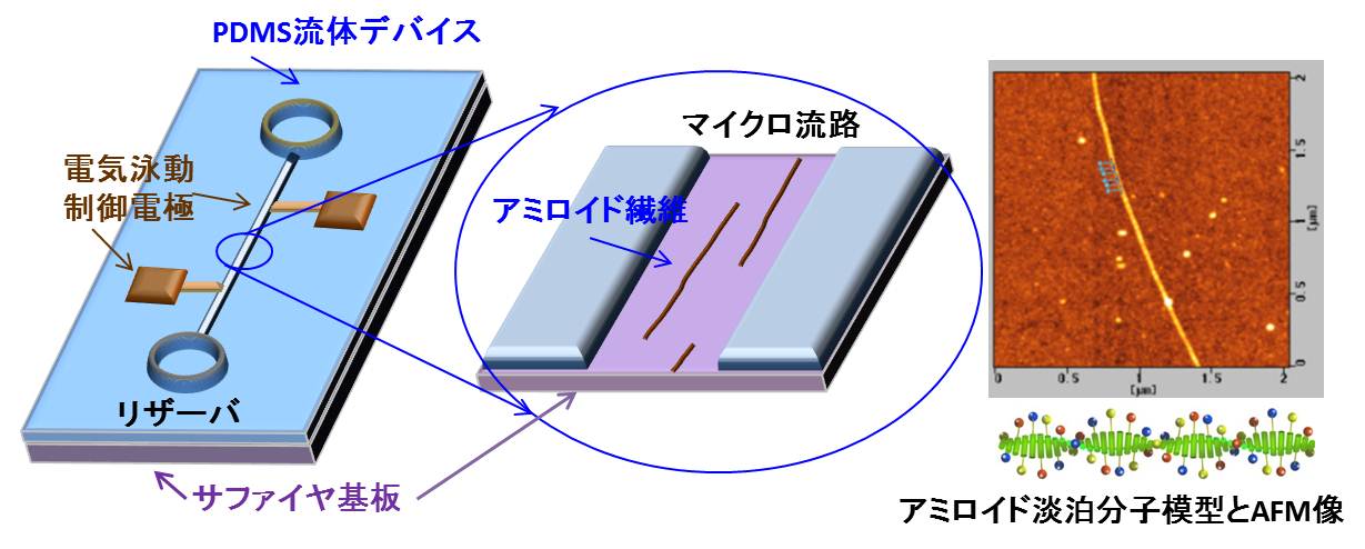
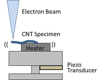
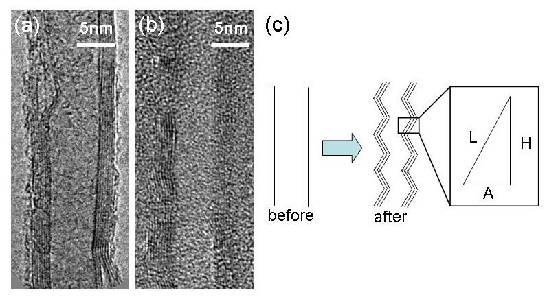
1.3 Three-dimensional nanoporous graphene Three-dimensional (3D) nanoporous graphene with preserved 2D Dirac electronic characters was successfully synthesized. The nanoporous graphene is constructed by a single layer graphene sheet that is continuously inter-connected to form a complex 3D network structure. This free-standing nanoporous graphene with an excellent crystallinity possesses high electron mobility, holding great promise for the applications in electronic, optic and energy related devices. The nanoporous graphene were grown by a nanoporous metal based chemical vapor deposition (CVD) method in Figure (a). The overall morphology of the nanoporous graphene in Figure (b) shows a ~20 μm thick free-standing bulk sheet. Although the 3D nanoporous graphene has a complex structure, it is demonstrated to be ~5000 cm2/Vs in electron mobility and a mass-less Dirac cone system. As the conventional transistor requires electron mobility of 200 cm2/Vs, it is greatly expected that this nanoporous graphene will bring new 3D graphene devices. 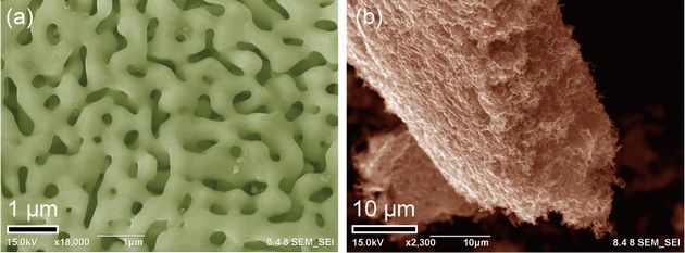 Figure (a) Nanoporous graphene on nanoporous Ni and (b) nanoporous graphene after dissolving the nanoporous Ni substrate. References: Yoshikazu Ito, et al. High Quality Three-Dimensional Nanoporous Graphene, Angew. Chem. Int. Ed. 2014, 126, 4822-4826. (Hot Paper). 1.4 Three-dimensional nanoporous graphene for hydrogen evolution Three-dimentional (3D) nitrogen(N) and sulfur(S) co-doped nanoporous graphene with preserved high conductivity was successfully synthesized. The 3D NS-doped nanoporous graphene is constructed by a few layer graphene sheets that are continuously inter-connected to form a complex 3D network structure. Due to the nitrogen and sulfur co-doping and abundant nanoporous structures, the catalysis towards hydrogen evolution reaction has been successfully activated inside and outside the nanoporous graphene at absence of any metal catalysts. This hydrogen harvesting technology with 3D metal-free graphene catalyst shows a great promise for achieving economic hydrogen energy at high efficiency for green energy innovation. 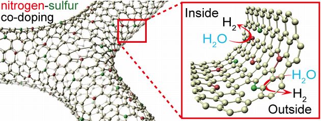 Figure Metal-free chemically doped three dimensional graphene electrode for hydrogen evolution. References: Yoshikazu Ito, et al. High Catalytic Activity of Nitrogen and Sulfur Co-Doped Nanoporous Graphene in the Hydrogen Evolution Reaction, Angew. Chem. Int. Ed. 2015, 54, 2131-2136. 3D nanoporous graphene electrode for hydrogen production 2. CNT Super Capacitor Main energy resource of the next generation would be renewable energy, such as solar energy, wind energy, wave power, geothermal energy. But the efficiency of this renewable energy is rather unstable that strongly depended on the unpredictable fluctuation essentially existed in the natural environment, in contrast to the quite stable power supplying realized in the nuclear and thermal power system.Therefore, we need an effective storage system of the power and the precise control to balance supply and demand. Extreme shrinkage of CNT is one of our creative findings that will progressively improve the maximum storage capacity of CNT based supercapacitor for the key device of power storage.Carbon nanotube has, as its name suggested, very thin diameter and nice conductivity.Due to the extremely thin diameter, the total surface area for each unit weight and/or unit volume has greatly large area about 2000 m2/g. This surprisingly large area could be useful for the electrode to realize grate capacitance. The structure of supercapacitor is quite simple. Since an electrical double layer was induced on the CNT surface when it was immersed into an electrolyte, thus one can easily constructed the supercapacitor using a thin film of ion-permeable membrane sandwiched by positive and negative CNT electrodes. However, researcher reported that the CNT based supercapacitor almost reached to the theoretical limit, if one utilizes the CNT as it is. Finding out how to break through the current limitation would be the great pleasure for our engineers and scientists. Someone try to make worm holes on the side of CNT body to use the inside wall, but the maximum enlargement could not be exceed the factor of 2. In contrast, our strategy is to use shrunk CNT for the supercapacitor electrode. We found that a CNT showed extreme shrinkage when a CNT was irradiated low energy of electron shower with a slight tensile stress that was induced by supersonic vibration, and the maximum shrinkage of 90% was observed. However, the diameter of the shrunk CNT thicken the diameter a little bit, thus the totally enlargement of the surface area for unit volume will be in about 600% to 700%.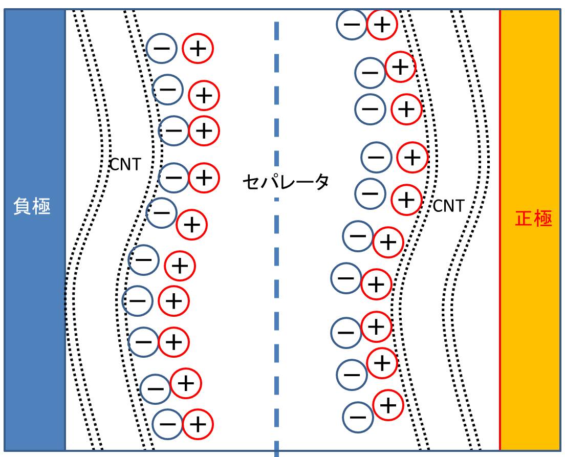
3. Construction in TEM Fundamental factors to characterize various properties of material would be microscopic shape of the material and its atomic lattice structure. In order to explore and to construct an artificial carbon nano structure under in-situ TEM observing filed, we build up our original nano-manipulator that can be operated in the TEM specimen holder, combining with the ultra-spurned probe that describes in following chapter 4. Based on the comprehensive understanding of the carbon nanostructure in terms with its electrical and mechanical properties from the view point of atomic level resolution, we would like to challenge to create functional carbon nano structures and/or artificial molecules for the future electrical application. 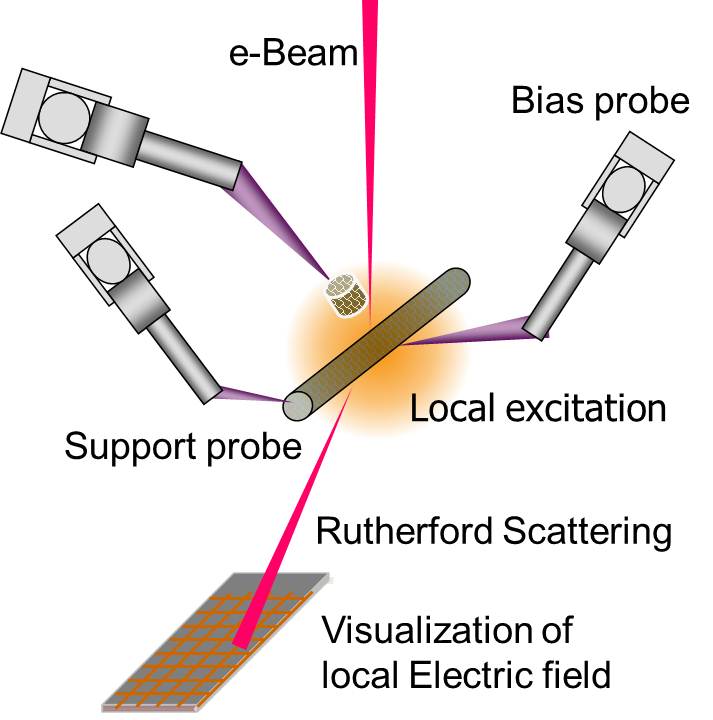
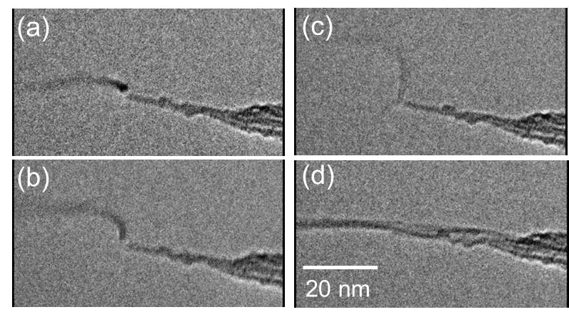
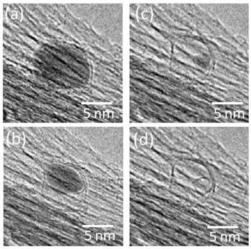
3.1 Artificial carbon nano-structure We demonstrated to construct an artificial carbon nanostructure controlling a dynamic transformation of carbon hexagonal lattice that was induced by a Joule heating and a local field emission. For example, Joule heating to a pair of DWNT induced a connection of them self, if the contact was prepared by a flesh cutting edges. Bended CNT was also recovered to a straight one by Joule heating. When an iron particle that was encapsulated in a multi-walled carbon cage (a) was Joule heated, some of internal cages was absorbed into the particle (b), and the iron particle was ejected with opening a hole at the end of the cage (c) in a short instance, and finally the outer carbon cage was artificially deformed and enlarged by a slight share force (d). 
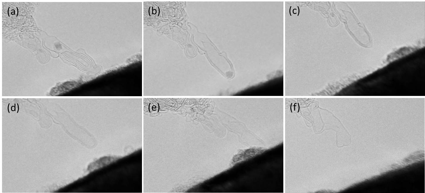
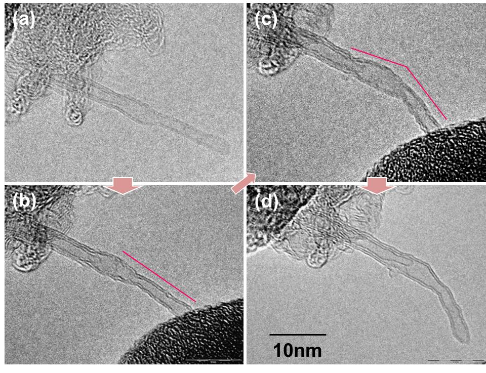
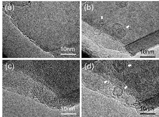
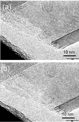
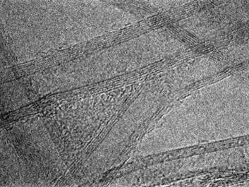
3.2 Pulse induced fullerene We found a new cage transformation process where a cyclic current pulse strongly triggered and enhanced the transformation of the cages from amorphous carbon that adhered on graphene sheet. We utilized very thin graphite sheet, which included about 10 to 30 stuck of graphene that embedded on a copper mesh. It should be noted that if we applied DC current on the graphite fragment via tungsten probe, local Joule heating of the fragment cleaned up the surface contamination, but, neither fullerenes nor carbon cages were produced on the surface except the contrast enhancement of the folding edge of the graphite. However, when we applied totally 10 pulses to the specimen with the cycle of 20 msec., the pulse train produced many fullerenes and cages on the surface. Additional current pulse never generated fullerenes on the graphene surface cleaned by DC Joule heating, thus we think that the amorphous carbon would the probable source of fullerene. We think that constructing functional nanostructures of carbon base material can be possible using our new approach based on pulse heating technique. 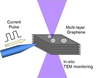
3.3 Mechanism of Ga catalysis Metal catalysts such as nickel and iron have a finite solubility of carbon, thus the carbon atom that dissolved into the catalyst could be segregated and crystalized for both nanotube and graphene growth at a specular position on the metal. In contrast, carbon insoluble metal, typically as copper, is well known to act as a superior catalyst for graphene growth. For the same metallurgic fashion of carbon insoluble metal, we had reported that liquid gallium has adequate ability to form very thin graphene layers at the interface between liquid gallium and amorphous carbon. We found that gallium nano-droplet has a finite solubility of carbon via in-situ transmission electron microscope (TEM) observation, thus graphite onions were produced around the droplet during evaporation by Joule heating.We think the detailed understanding of the catalytic mechanism of liquid Ga give us an essential way how to produce a large area graphene with small defects. 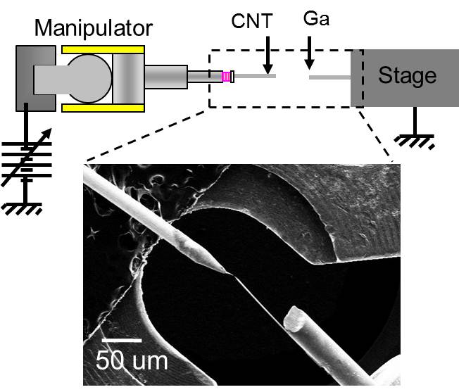
 Basic Technologies
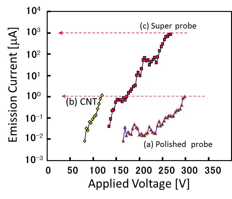
4. Ultrashrp probe We developed an ultrasharp tungsten probe that has about 2 nm of the radius of curvature. By controlling the field emissions from a multiwalled carbon nanotube that embedded on a conventional electropolished tungsten probe, the Joule heating soften the tip of the tungsten probe, in addition, the Coulomb attraction to the nanotube finery pulled from the tungsten tip, resulted in an ultrasharp apex of the tungsten probe. This ultrasharp tungsten probe remarkably decreased the threshold voltage of the field emission from the tip, which was almost the same with that of CNT. We our laboratory utilized the ultrasharp tip as the key device for SEM/TEM nano-manipulation. 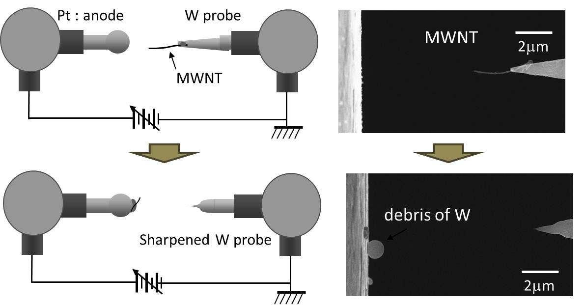

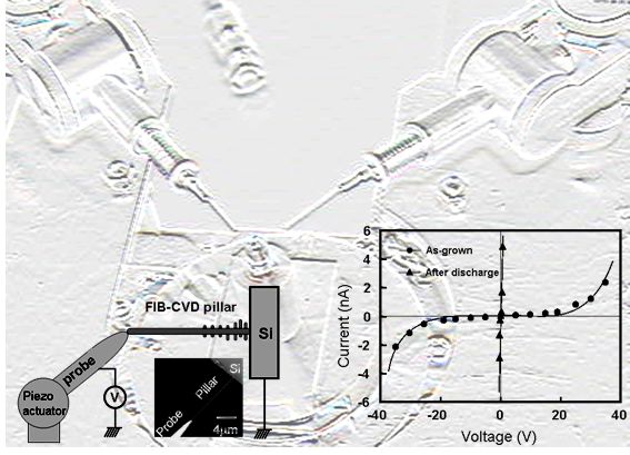
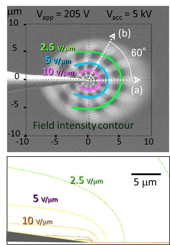
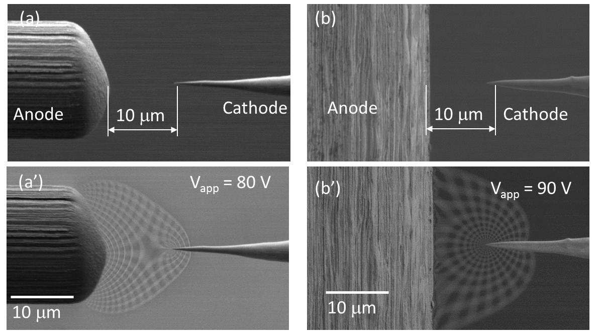
5. Visualization of local E-field We also found that a local electric field at the probe apex can be visualized in an imaging filed of scanning transmission electron microscopy STEM, when it operated at a low accelerating voltage around 5 keV. This local electric field that was induced around the probe apex deflected the primary electron beam of the STEM, producing a dark circular shadow surrounding the probe apex in the STEM image. We analyzed the distribution of this local field using a simple Rutherford scattering model. We also demonstrated an in-situ visualization and 2D mapping for a local electric field using a conventional SEM system combined with a grid detector under a low acceleration voltage of 5 keV. The square shape of the cross grid was projected as concentric rings and radial spokes that appeared to superimpose immediately behind the conventional SEM image. The obtained 2D electric field distribution agreed well with the FEM simulation. These results suggested that our in-situ visualization technique would not only be useful for determining the local field enhancement behavior for various geometrical configurations and apex shapes, but this detection principle would also be applicable to the analysis of device operation in a nanoscale structure combined with a conventional STEM system. 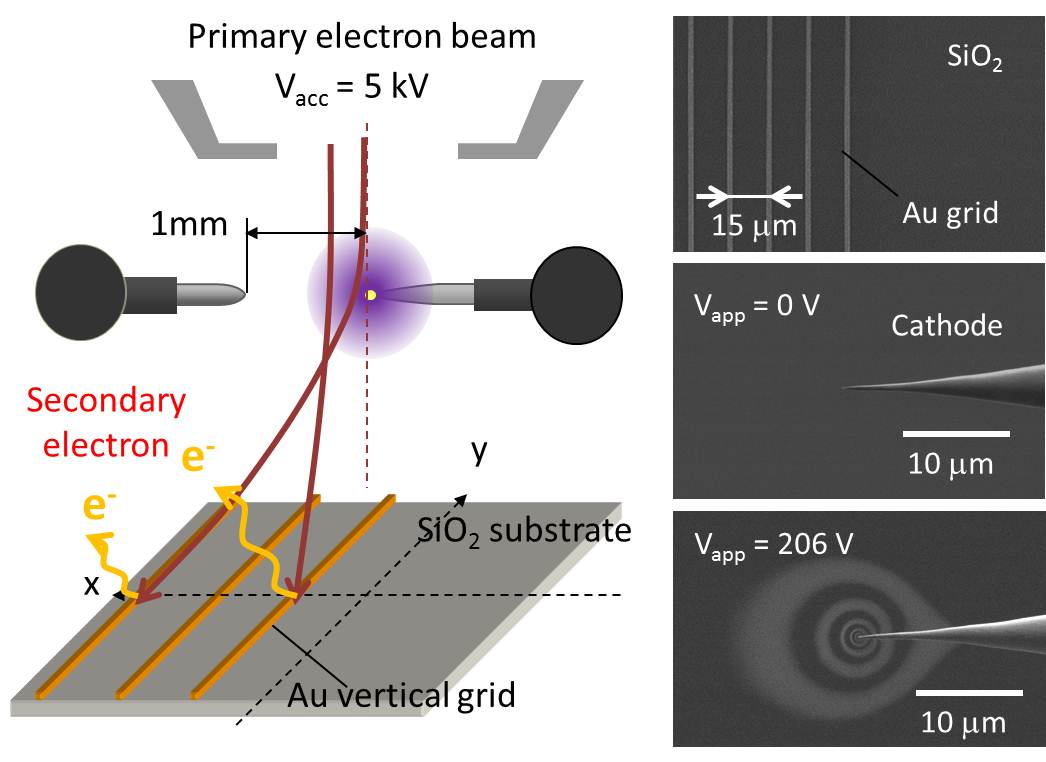
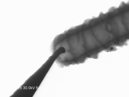
6. EB/CVD technique The focused ion-beam-induced chemical vapor deposition (FIB-CVD) technique has the profound advantage of enabling the construction of real three-dimensional (3D) structures. Even though the beam is always incident perpendicular to the point of deposit, depositions grow horizontally, forming an overhanging structure. We previously reported the production of three-dimensional plastic art with amorphous carbon, in wine glass and coil shapes, which were fabricated using a FIB-CVD technique with phenanthrene source gas. The basic mechanism for 3D growth with FIB-CVD results from the shallow depth of the primary Ga ions in the area of deposit, as shown in the left figure. Primary Ga ions of 30 keV typically penetrate the amorphous carbon to a depth of about 20 nm. This area of penetration is spherically distributed beneath the growth point. The growth of the amorphous carbon seems to combine indirectly with the primary ions, but appears to be strongly dominated by the secondary electrons emitted by the inelastic scattering process of the primary ions. 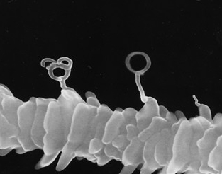
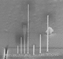
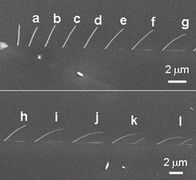
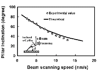
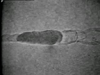
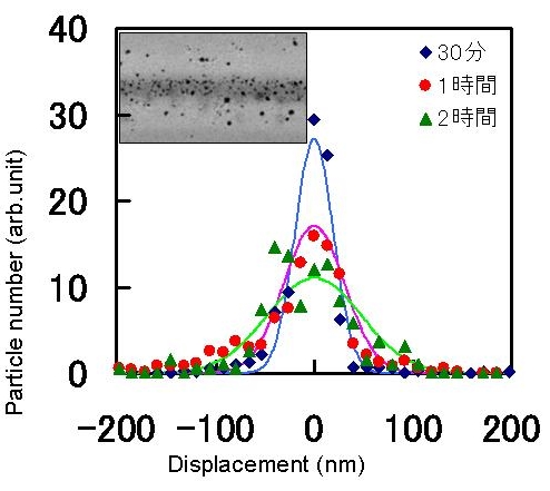
7. Carbon nanotube (1)Position controlled CNT growth We demonstrated nanotube growth on a position-controlled catalyst using electron beam induced chemical vapor deposition (EB-CVD) ferrocene pillars. While solid phase graphitization was induced at 650 oC, the iron nano-particles only appeared on the surface by eroding the surrounding graphite triggered by the gas phase carbon fiber growth, at a temperature of over 800 oC using ethanol vapor. The precise position control in the EB-CVD method would be useful for future device applications. (2)in-situ obsrvation of CNT solid phase growthWe show a clear evidence of solid-phase nanotube growth where traces of iron nano-particles were graphitized in an amorphous carbon nano-pillar fabricated by electron beam induced chemical vapor deposition (EB-CVD). The random walk of iron particles in the carbon nano-pillar caused continuous growth of wavy graphite tubes behind the iron particles as they moved during vacuum annealing at 800 C for 30 min. The graphite sheet in this solid-phase graphitization seemed to be produced at the tail of the iron nanoparticles, and some of the graphite tubes were multi-wall ones containing bamboo-joint-like cap sheets. (3)Control of the diffusion of iron particleSolid-phase graphitization, and thus solid-phase nanotube growth, was induced by the movement of iron particles into an amorphous carbon matrix at a certain temperature around 600 C. We analyzed this iron particle movement in an amorphous carbon wall by in situ monitoring by scanning transmitted electron microscopy (STEM). Isotropic diffusion of iron particles with a diffusion constant of approximately 0.06 nm2/min at 680 oC during furnace heating was observed. In contrast, during anisotropic heating, which was realized by heating a wall-shaped specimen on a fine tungsten filament, the Gaussian distribution of the iron particles shifted toward lower temperature. Iron particles in solid-phase graphitization preferred to move to a lower temperature region, where an exothermic reaction can catalyze amorphous carbon into graphite. (4)Catalytic reaction of GaWe found that a flash motion of Ga droplets with Joule heating transformed an amorphous carbon pillar into multiwalled carbon nanotube. Flush discharge into the pillar quickly heated up Ga droplets, which originally incorporated in the pillar due to the fabrication technique with focused-ion-beam-induced chemical vapor deposition, inducing a flash motion of Ga toward negative electrode. Thus, the Ga droplets dug out a tunnel inside the pillar, simultaneously inducing a catalytic transformation into a multiwalled graphitic tube. 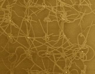
Projects and Funds Funds
ProjectWe also promote the collaboration with company.
|
|
Copyright © Fujita-Ito Lab. All rights reserved. http://www.bk.tsukuba.ac.jp/~nanofab/index.html |