|
Fujita-Ito Lab. GraduateSchool of Pure and Applied science Institute of Applied Physics, University of Tsukuba |
>>>Japanese |
Major facilities in Fujita-Ito Lab.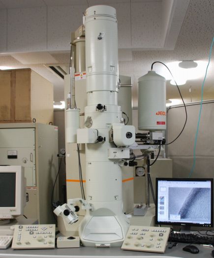 High resolution transmission electron microscope (JEOL JEM2100) 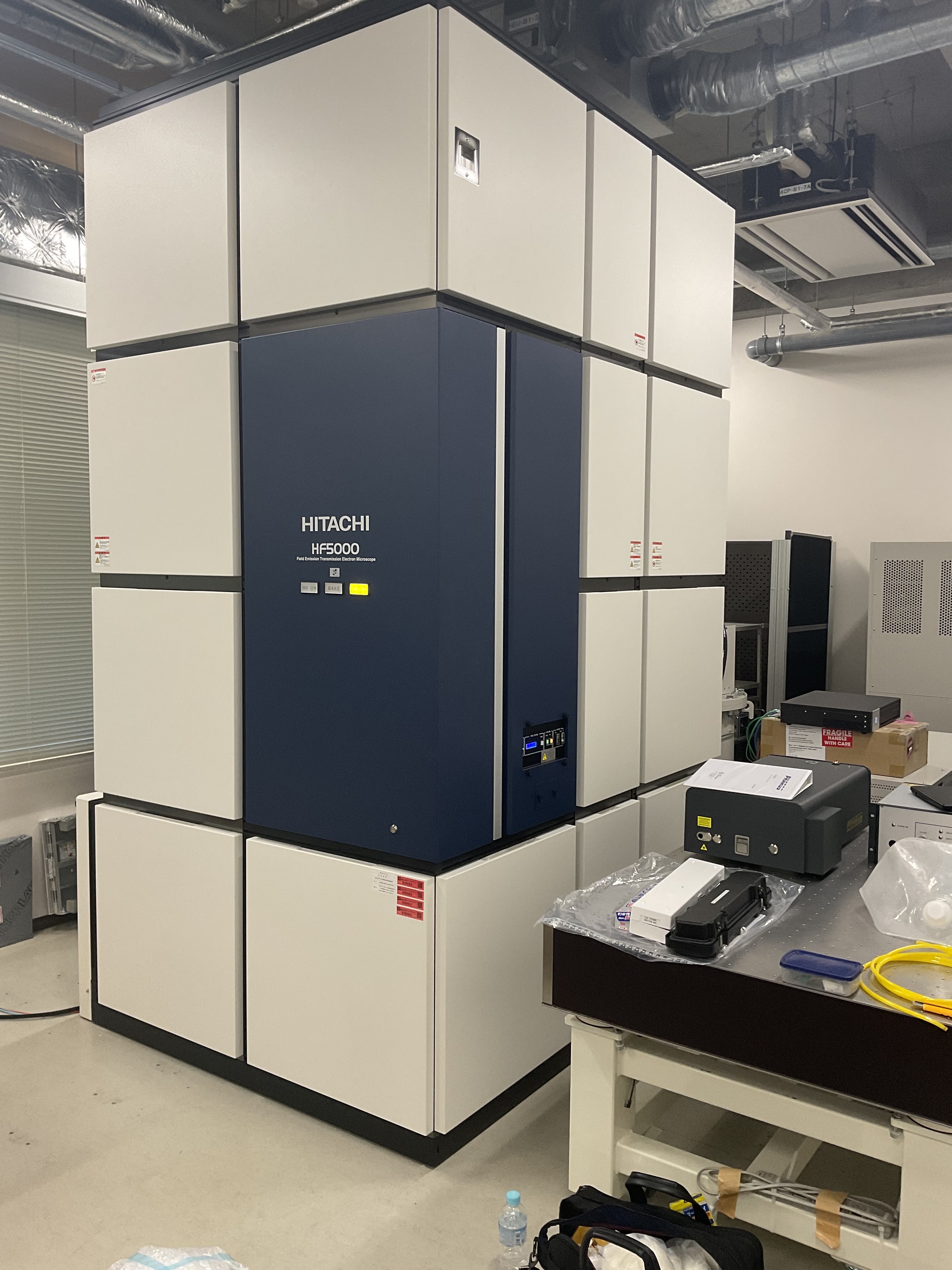 Field Emission Transmission Electron Microscope (HITACHI HF5000) 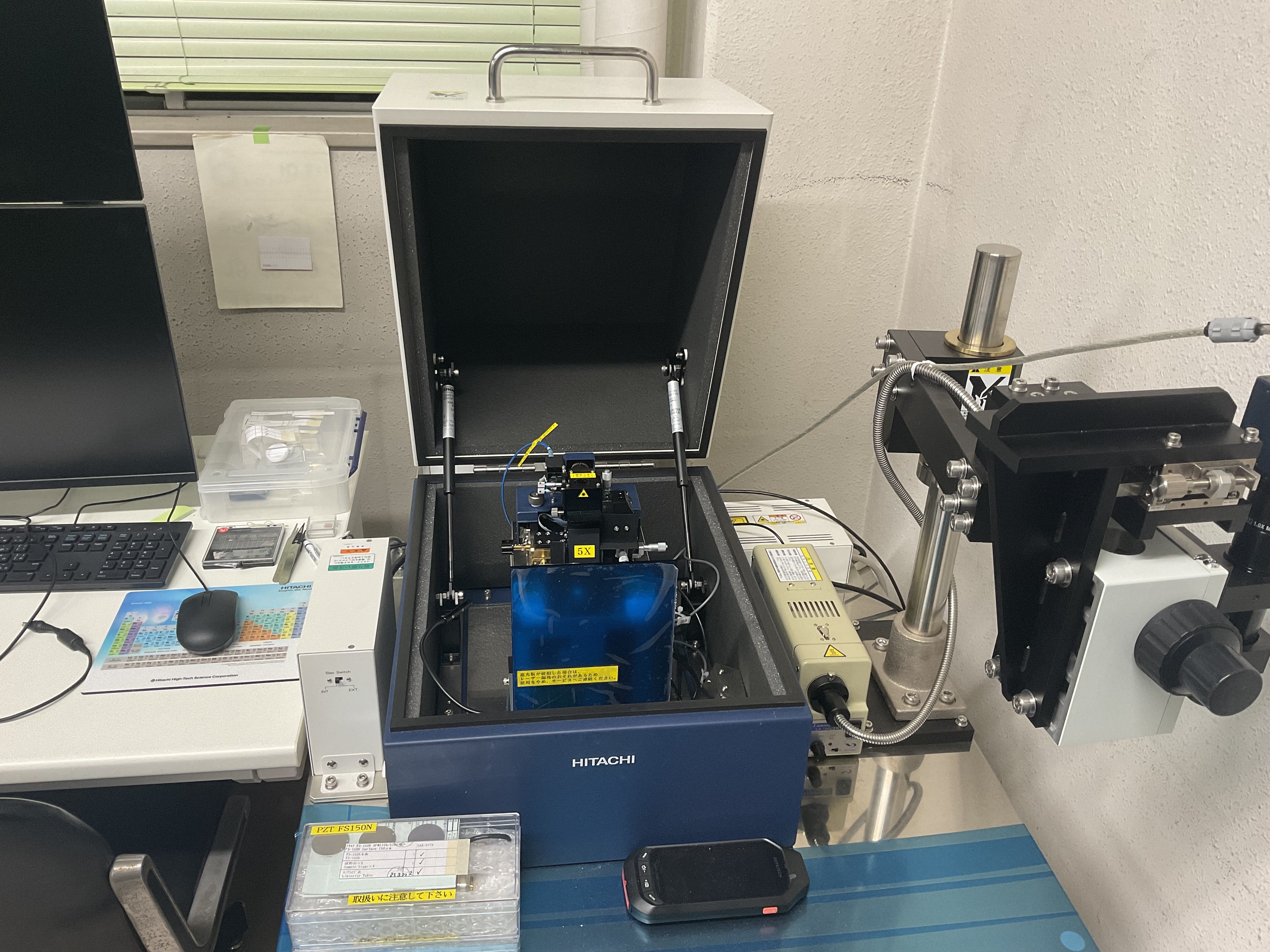 Atomic Force Microscope (HITACHI AFM-5200S) 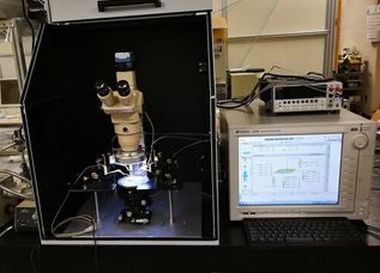 Semiconductor Device Parameter Analyzer (Keysight B1500A) 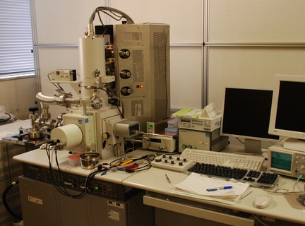 Electron Beam Writer Based on Hitachi S4300SE, very stable emission from athermal field emitter adapted with differential pumping system enables high-resolution pattern writing for nano-device fabrication process. 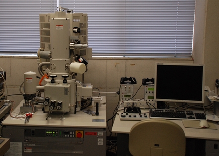 High resolution scanning electron microscope (Hitachi S4800) Using three nanomanipulator (Kleindike) in the specimen chamber, all of samples for our experiments was prepared in this HR-SEM system. 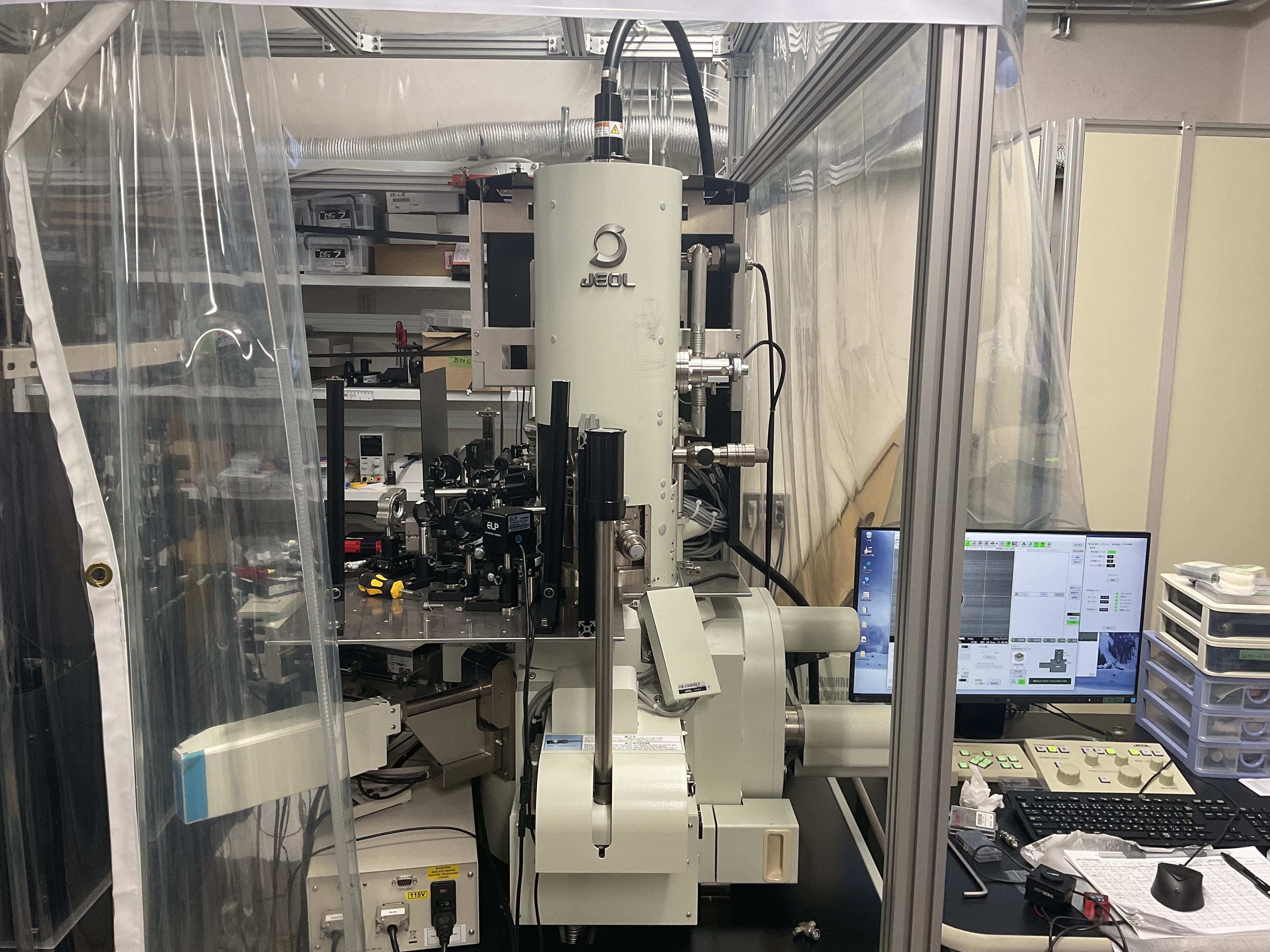 JSM-7200F Schottky Field Emission Scanning Electron Microscope (JEOL JSM-7200F) 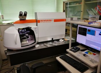 Raman microscope (Renishaw) 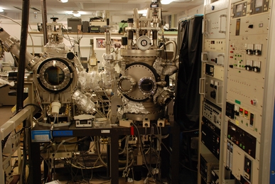 Ion milling and Laser ablation system This system is used for thin film preparation by pulsed YAG laser,and nano-pattern was procedded with micro-wave activated Ar ion beam. 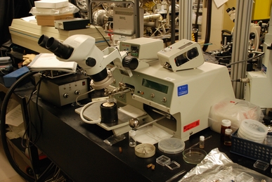 Wire-bonder (WestBond) fabricated nano-device was mounted on LSI dip-package with Au wiring. 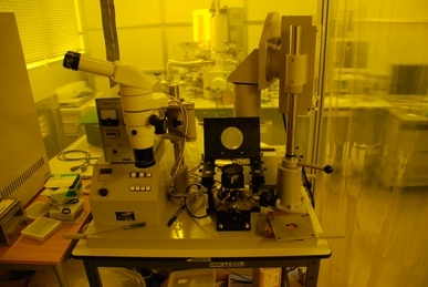 Mask aligner This yellow curtain blocks the ultra vaiolet against the pattern exposure, under cleen environment of about Class 1000 atained by dual HEPA filters. 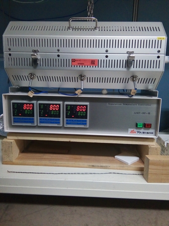 CVD Equipments(Made in Labo) 2D,3D graphene,Carbon Nanotube and Nanoporous structure made from MoS2 are produced by these equipments. There are 8 equipments which are assigned for each graduate and doctor student. 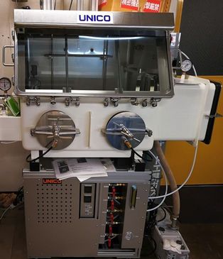 Vacuum Glovebox (Unico) Provide a controlled environment that protects contamination-sensitive materials from ambient conditions such as oxygen and moisture. 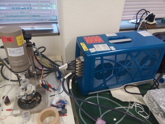 ElrctroChemical Measurement System (Unico) Battery Characteristics,Electrode Reaction,Electrolytic Corrosion and Super Capacitor are measured with high precision. Measurement Channels are assigned for each graduate and doctor student. 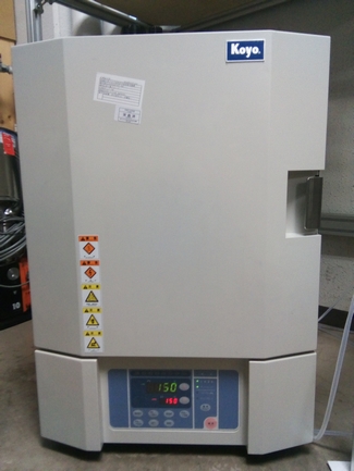 Box type Electric furnace (Unico) Used for heating process under 1000℃ such as hydrothermal synthesis by an autoclave. 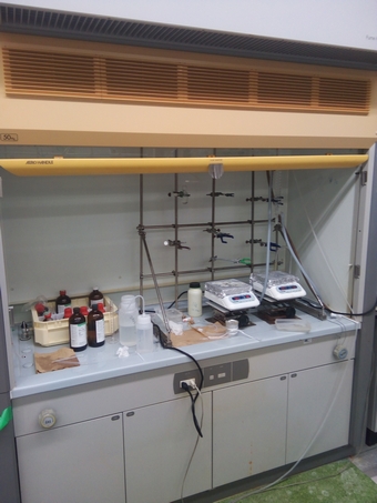 Draft Chamber (Unico) Chemical is treated in this equipment. |
|
Copyright © Fujita-Ito Lab. All rights reserved. http://www.bk.tsukuba.ac.jp/~nanofab/index.html |